Black phosphorus atomic structure diagram, folded honeycomb structure In recent years, two-dimensional crystal materials have become a new direction for semiconductor materials research because of their superior electrical properties. Following graphene and molybdenum disulfide, this month, in the journal Nature Nanotechnology, Prof. Zhang Yuanbo from the Department of Physics at Fudan University discovered a new type of two-dimensional semiconductor material, black phosphorus, and successfully prepared the corresponding Field-effect transistor devices, which will likely replace traditional silicon, become the basic material for electronic circuits. A two-dimensional crystal is a nanometer-thick planar crystal in which several layers of monoatomic layers are stacked, such as the famous graphene, but graphene has no semiconducting bandgap, ie, separate electronic conduction bands (conducting bands) and non-conducting bands ( The uninhibited area between the valence belts means that it is difficult to complete the conversion between the conductor and the insulator, and the logic of the digital circuit cannot be turned on and off. Black phosphors, which are also stacked by a single atomic layer, have a semiconductor bandgap. “When Professor Chen Xianhui of the China University of Science and Technology told me two years ago that they could grow black phosphorus, at that time intuition told me that it could be a good semiconductor material,†said Professor Zhang Yuanbo. “Sure enough, now we do the black phosphorus. After the nanometer-thick two-dimensional crystal is formed, it is found to have very good semiconductor properties so that it can be used in future integrated circuits." They found that black-phosphorus two-dimensional crystals have good electron mobility (~1000 cm2/Vs) and very high leakage current modulation (10,000 times that of graphene), similar to the traditional material silicon of electronic circuits. In addition to its superior electrical properties, the optical properties of black phosphorus also have significant advantages over other materials including silicon and molybdenum sulfide. Its semiconductor bandgap is a direct bandgap (as shown in the figure). That is, the bottom of the electronic conduction band (the conduction band) and the top of the non-conducting energy band (the valence band) are at the same position. From non-conduction to conduction, electrons only need to absorb energy. (Light energy), while conventional silicon or molybdenum sulfide are all indirect band gaps, requiring not only energy (band changes) but also momentum (position change). This means that black phosphors and light can be coupled directly, a feature that makes black phosphors an alternative material for future optoelectronic devices (eg, photosensors) that can detect the entire visible to near-infrared spectrum. These preliminary results are far from the limit of black phosphorus performance, and there is still much room for development. Prof. Zhang Yuanbo said that black phosphorus is just a material that has just been discovered, and it is still too early to make any predictions about its prospects. “Many properties of this material have yet to be explored. Our laboratory will continue to explore these features and hope to further improve the quality of the samples on the basis of the present.†Professor Zhang Yuanbo said, “Another thing we are trying is to see Can you dissociate the black phosphorus from the monoatomic layer? What is the different nature of the black phosphorus in the monoatomic layer? No one knows yet." Smart Faucet,Smart Faucet Price,Smart Faucet Product Yuyao Zelin Sanitary Ware Co., Ltd , https://www.zelinsinkfaucet.com
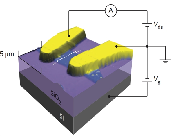
Black phosphorus two-dimensional crystal field effect transistor structure diagram 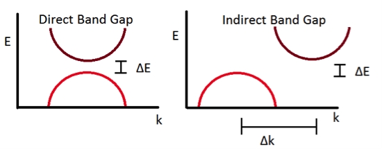
Direct Bandgap (Left) and Indirect Bandgap (Right) Band Profiles
Black phosphorus will be another new two-dimensional semiconductor to replace silicon